555 LED blinker
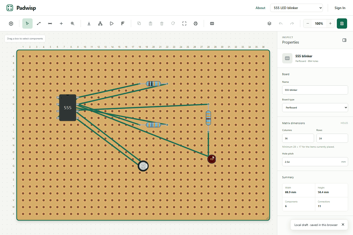
Explore timing with a 555 timer, resistors and a capacitor. Change a value and compare the waveform.
Open in editorPlan, understand and build perfboard and stripboard circuits in your browser. Put every part and connection in place before you pick up the soldering iron.
No account needed to edit, simulate or download a backup.
A circuit is more than a drawing. Follow the connections all the way to the build.
Choose a board, add components and rotate them onto the hole grid. Use perfboard or horizontal or vertical copper strips.
Trace connected pads, add wires and solder paths, and cut strips where needed. Generate a schematic from your board’s actual connections.
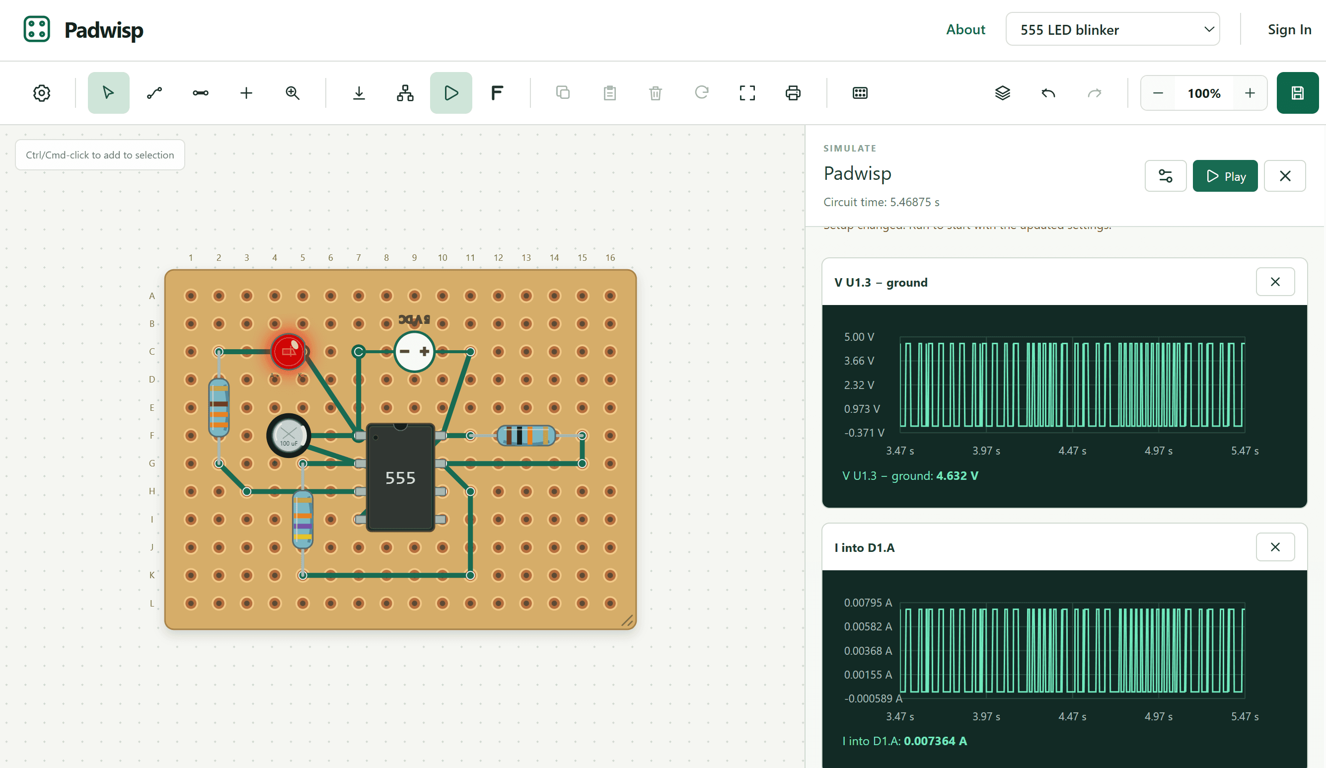
Configure a voltage source, choose probes and watch voltage and current traces. Check what changes when you edit a component value.
Open Build guide for the parts list and mirrored solder-side SVG. Print at actual size and check the 50 mm scale before building.
Three editable examples. Open one without signing in, then explore its parts and wiring.
Explore timing with a 555 timer, resistors and a capacitor. Change a value and compare the waveform.
Open in editorFollow the base, collector and emitter connections and explore how a transistor switches an LED.
Open in editorExplore low-voltage AC, diode polarity and capacitor smoothing. Use an isolated low-voltage source for a physical build, never mains.
Open in editorThese are editable example projects. Physical build reports and full guided tutorials are still to come.
Try this short exercise with the 555 blinker:
For component tutorials, select a part and open its guide in Properties. Try the transistor switch next.
Built-in simulation supports modeled analog components and 555 circuits, plus supported behavioral device models. It uses your board’s connections. Unsupported parts, invalid values or missing references can prevent a run.
Models simplify real devices. Simulation and schematic drawing verification do not guarantee a working physical circuit or check every rating, tolerance, thermal effect or assembly mistake. Verify your parts and test the physical build.
Editing, simulation, JSON backups and build exports are available without an account. Browser recovery helps resume work on this device, but clearing browser data can remove it. Download a backup for a copy you control.
An optional account lets you keep private cloud projects and reopen them after signing in. Save your guest work from the projects dashboard. Examples are starting points; edits to your copy do not update the original example.
Open your projects